

Introduction
Flex PCB cost depends on many design and manufacturing choices. Materials, layer count, board size, copper thickness, hole size, surface finish, and stiffeners can all raise the price. Understanding these cost drivers early helps you build a reliable flexible PCB while avoiding unnecessary processing, wasted material, and preventable manufacturing costs.
Flex PCB Cost Drivers at a Glance
Some design choices require premium materials, special equipment, or additional production steps. Others reduce manufacturing yield and increase scrap. The following table summarizes the main flex PCB cost drivers and practical ways to control them.

| Cost driver | Why it increases cost | How to reduce the cost |
|---|---|---|
| Material selection | Special flex materials cost more | Use standard materials that meet product requirements |
| Layer count | Each layer adds material and production steps | Use only the layers the design needs |
| Board size and shape | Unusual shapes waste panel space | Improve the outline and panel layout |
| Trace width and spacing | Small features need tighter process control | Use standard trace and spacing sizes |
| Copper thickness | Special or thick copper costs more | Specify only the thickness required |
| Drilled-hole size | Small holes are harder to drill | Use standard hole sizes where possible |
| Drill-to-copper clearance | Tight gaps increase defect risk | Leave more space around holes |
| Surface finish | Premium finishes add processing | Match the finish to the application |
| Stiffeners | Add material and bonding work | Use standard materials and thicknesses |
| Manufacturing yield | Complex boards create more scrap | Follow standard rules and request DFM review |
Top 10 Cost Drivers of Flex PCBs
Flex PCB pricing reflects the board type, materials, stack-up, drilling, finish, and mechanical reinforcement. HDI and every-layer interconnect structures cost more because they require additional imaging, lamination, drilling, and inspection.
1. Flex PCB Material Selection
Polyimide is the most common material for flex cores and coverlays. It offers good thermal stability and flexibility for repeated bending and higher operating temperatures.
Adhesive-Based Versus Adhesiveless Laminates
Adhesive-based laminates bond copper to polyimide with an adhesive layer and are typically more economical. Adhesiveless cores bond copper directly to polyimide. They cost more, but can make the circuit thinner while improving heat resistance and plated-hole reliability.
Factors Affecting Material Selection
Choose materials according to operating temperature, physical stress, bend radius, signal speed, and impedance. Avoid performance the product does not need. The official IPC board design standards provide useful context.
2. Layer Count and Stack-Up Complexity
Each added layer needs more material, imaging, alignment, lamination, inspection, and testing. More layers also increase the risk of registration errors and lamination defects. Review routing density before moving to a multilayer flex PCB.

| Layer increase | Estimated cost increase |
|---|---|
| 1 to 2 layers | 35%–40% |
| 2 to 4 layers | 35%–40% |
| 4 to 6 layers | 30%–40% |
| 6 to 8 layers | 30%–35% |
| 8 to 10 layers | 20%–30% |
| 10 to 12 layers | 20%–30% |
Actual prices depend on design, materials, quantity, and manufacturer capabilities.
3. Board Size, Shape, and Panel Utilization
Larger flex PCBs consume more material. Squares and rectangles generally nest efficiently, while circles, long arms, and irregular shapes can leave unusable panel space.
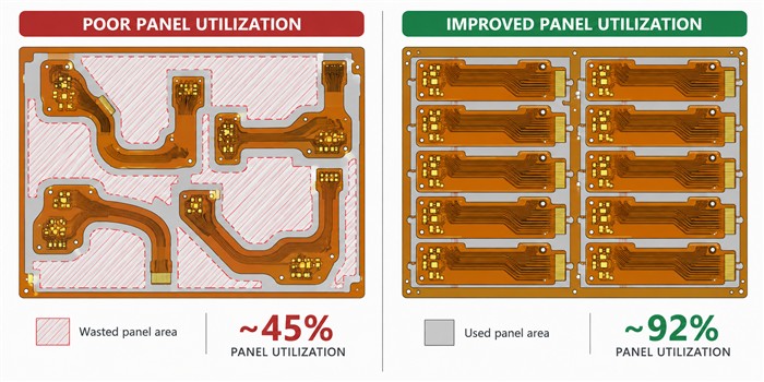
Good nesting allows more circuits to fit on each panel, lowering material cost per board. Ask the manufacturer to review panel utilization before finalizing the outline.
4. Trace Width, Spacing, and Tolerances
Very small spaces are harder to etch and increase the risk of shorts, opens, or damaged pads. Tight tolerances require more process control and inspection. Use standard rules whenever possible to improve yield.
5. Copper Type and Thickness
Thicker copper increases material and processing costs and requires wider traces and larger spacing. Very thin copper may also need special processing. Specify only the copper weight required for current, heat, and bending performance.
6. Drilled-Hole Size
Small holes take longer to drill and may require special tools or laser drilling. Confirm preferred drill sizes with the manufacturer before completing the layout.
7. Drill-to-Copper Clearance
This is the distance between a drilled hole and the nearest pad, trace, or copper area. More clearance improves manufacturability and reduces the risk of cutting into adjacent copper.
8. Surface-Finish Selection
A surface finish protects exposed copper and creates a solderable area. Choose according to soldering, storage, reliability, flatness, and application requirements.
Common Surface Finishes
- ENIG: Reliable and tarnish-resistant, but usually more expensive.
- Immersion silver: Flat and suitable for many applications.
- Immersion tin: Flat and economical, with a shorter shelf life.

9. Stiffener Material and Construction
Stiffeners support connectors and components and provide mechanical reinforcement. FR-4 and polyimide are common; aluminum and stainless steel are more expensive. Standard materials, simple shapes, and uniform thickness reduce fabrication time. Learn about flex PCB stiffener options.
10. Manufacturing Yield and Production Volume
A late-stage defect wastes all earlier material and processing. Low-volume orders also cost more per board because engineering, tooling, testing, and validation costs are divided across fewer units.
How to Minimize Flex and Rigid-Flex PCB Costs
Reducing flex and rigid-flex PCB cost starts during design. A simpler design uses less material, fewer process steps, and has a lower defect risk.
Keep the Layer Count Low
Use only the layers needed for routing, power, ground, and signal control, without compromising electrical or safety requirements.
Use Rigid Materials for Thickness
Where appropriate, lower-cost rigid laminates can build thickness in rigid-flex areas. Keep the stack-up balanced and request a manufacturer review.
Improve Panel Utilization
Keep the outline compact and avoid long arms, curves, or empty regions that serve no function.
Maintain Uniform Stiffener Thickness
Use one standard thickness where possible and favor common materials such as FR-4 or polyimide.
Limit Advanced Vias
Blind, buried, stacked, and laser-drilled microvias add specialized drilling, plating, and lamination. Use through-holes when space allows.
Request an Early DFM Review
Discuss materials, holes, traces, spacing, finish, and stiffeners before design release. The IPC-2223 flexible and rigid-flex design standard overview is a useful reference.
Conclusion
Flex PCB costs can be reduced through practical design decisions: use fewer layers, improve panel layout, specify standard materials and features, keep stiffeners consistent, and avoid advanced vias unless they add clear value.
Work with the manufacturer early to review materials, stack-up, design rules, and production volume. For project-specific guidance, contact MV Flex Circuit for a DFM review and quotation.


