

Introduction
Selecting the right SMD diode package is an important part of PCB design. As one of the most commonly used circuit board components, diodes come in various package shapes and sizes tailored for specific applications. Choosing the right one helps save space, manage heat, support soldering, and keep the circuit working safely.
What Are SMD Diode Packages?
SMD diode packages are compact housings designed to mount diodes directly onto the surface of a printed circuit board. Unlike through-hole components, they do not require leads to pass through drilled holes, making them suitable for automated assembly and high-density PCB layouts.
The package protects the semiconductor die from moisture, dust, mechanical stress, and heat. It also provides metal terminals that connect the diode electrically and thermally to the PCB. Packages vary in body shape, dimensions, terminal arrangement, and heat-dissipation capability.
It is important to distinguish between the diode, its package, and its PCB footprint. The diode is the electronic device that controls current flow, while the package is its physical enclosure. The footprint is the arrangement of copper pads used to solder that package onto the board.

Main Types of SMD Diode Packages
SMD diodes are available in several package styles, each designed for particular electrical, thermal, and space requirements. The main differences include body shape, terminal arrangement, mounting area, power-handling capability, and ease of assembly.
Leadless Cylindrical Glass Diode Packages
Leadless cylindrical glass packages are commonly known as MELF packages, meaning Metal Electrode Leadless Face. They have a cylindrical body with metal contacts at both ends and are mounted horizontally on the PCB.
MELF diodes offer good electrical stability, heat resistance, and reliability. Their glass body offers mechanical protection and helps maintain stable electrical performance. Environmental performance depends on the specific device design and sealing method used. Common versions include standard MELF and MiniMELF packages.
However, their rounded shape can make automated placement more difficult because components may roll or shift before soldering. For this reason, accurate pad design and placement control are important. MELF packages are frequently used for switching, voltage regulation, signal protection, and general-purpose rectification.

Rectangular Plastic Chip Diode Packages
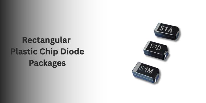
Rectangular plastic packages are among the most widely used SMD diode formats. Their flat surfaces provide better placement stability than cylindrical packages, making them well suited to high-speed automated assembly.
Common power-diode packages include SMA, SMB, and SMC. SMA is relatively compact and is often used for general rectification and transient-voltage protection. SMB is larger and can usually accommodate devices with higher current or power ratings. SMC provides an even larger body and is commonly selected for higher-power rectifiers, surge suppressors, and automotive circuits.
Smaller SOD packages, such as SOD-123, SOD-323, SOD-523, and SOD-923, are used where board space is limited. They are common in portable electronics, communication devices, sensor circuits, and compact protection networks. Although package size influences thermal performance, designers must always check the specific component datasheet because current and power ratings vary between devices.
Plastic-Packaged Composite Diodes
Composite diode packages contain two or more diode elements inside a single plastic enclosure. They may use common-anode, common-cathode, series, or independent internal connections. Many are supplied in three-pin packages such as SOT-23, although larger and smaller options are also available.
Combining multiple diodes in one package reduces component count and saves PCB space. It can also improve matching between diode elements because they are manufactured within the same device. These packages are commonly used for signal steering, logic circuits, power-input selection, electrostatic discharge protection, and high-speed switching.
Designers must carefully confirm the internal circuit and pin configuration because devices with identical package shapes may have different electrical arrangements.

SMD LED Packages
Surface-mount light-emitting diodes are packaged according to their physical dimensions, number of terminals, brightness, color configuration, and thermal needs. Common rectangular LED sizes include 0603, 0805, 1206, and larger high-power formats.
Small LED packages are widely used for status indicators, displays, keypad lighting, and consumer electronics. Multi-pin packages may contain red, green, and blue LED elements, allowing one component to produce multiple colors. High-power LEDs typically require larger thermal pads and more PCB copper to transfer heat effectively.

SMD Diode Package Size Chart
SMD diode packages range from extremely small signal-device formats to larger packages designed for rectification and surge protection. The dimensions below are approximate body measurements and may vary slightly by manufacturer. Always confirm the mechanical drawing and recommended land pattern in the component datasheet.
| Package | Approximate Dimensions | Typical Applications |
| SOD-923 | 1.0 × 0.6 mm | Ultra-compact signal and protection circuits |
| SOD-523 | 1.2 × 0.8 mm | Mobile devices and high-density PCBs |
| SOD-323 | 1.7 × 1.3 mm | Switching and small-signal diodes |
| SOD-123 | 3.7 × 1.6 mm | Zener, Schottky, and general-purpose diodes |
| MiniMELF | 3.5 × 1.4 mm | Precision switching and voltage regulation |
| SMA | 4.6 × 2.6 mm | Rectification and transient protection |
| SMB | 5.3 × 3.6 mm | Power supplies and surge suppression |
| SMC | 7.2 × 6.2 mm | Higher-power rectifiers and TVS diodes |
| SOT-23 | 2.9 × 1.3 mm | Dual diodes and diode arrays |
Smaller packages conserve PCB space but generally provide less surface area for heat transfer and may be more difficult to inspect or rework. Larger packages occupy more board area but can support improved thermal performance when combined with properly designed copper pads.
Key Considerations When Selecting an SMD Diode Package
Choosing an SMD diode package involves more than finding a component that fits the available board space. Designers must evaluate the diode’s function, electrical ratings, thermal behavior, footprint compatibility, and long-term availability.
Device Type
First, identify the type of diode required by the circuit. Rectifier diodes, Schottky diodes, Zener diodes, switching diodes, TVS diodes, and LEDs perform different functions and are available in different package families. The application determines the required switching speed, voltage drop, reverse-voltage capability, and protection level.
Package Type
The package should match the mechanical and thermal requirements of the design. Small SOD packages are suitable for compact, low-power circuits, while SMA, SMB, and SMC packages are often used for rectification and surge protection. Multi-diode devices may use three-pin SOT packages to save space and reduce component count.
Electrical Parameters
Check the diode’s maximum reverse voltage, forward current, surge-current rating, forward-voltage drop, leakage current, and power dissipation. For high-frequency circuits, reverse-recovery time and junction capacitance may also be important.
Polarity Orientation
Most diodes are polarized components, meaning the cathode and anode must be aligned precisely. Package markings can be miniature or obscure, making it vital to know how to identify smd components correctly during inspection and assembly. Clear PCB silkscreen symbols, updated land patterns, and standardized assembly documentation further prevent reversed placement defects.
PCB Footprint
The selected package must match the PCB land pattern. Similar-looking packages may have different body dimensions, terminal spacing, or recommended pad sizes. Designers should use the manufacturer’s mechanical drawing and recommended footprint rather than relying only on a general package name.
Replacement Risk
Two diodes in the same package are not necessarily interchangeable. Differences may exist in voltage, current, pin arrangement, thermal performance, and internal configuration. Availability should also be considered, particularly for products with long manufacturing lifecycles. Selecting widely supported packages and identifying approved alternatives can reduce redesign and supply-chain risks.
| Item | What to Check |
| Device type | General-purpose, Zener, switching, composite, or LED diode |
| Package type | Glass, plastic chip, composite, or SMD LED package |
| Electrical parameters | Rated current, voltage rating, power handling, forward voltage, and leakage current |
| Polarity orientation | Anode and cathode positions, LED positive and negative terminals, and composite diode internal connections |
| PCB footprint | Pad dimensions, component body size, and the recommended land pattern |
| Replacement risk | Identical packages may have different internal connections, so always verify the datasheet |
How SMD Diode Packages Affect PCB Assembly
The physical design of an SMD diode package influences PCB layout, automated placement, soldering quality, inspection, and long-term reliability. Selecting a suitable package can simplify manufacturing and reduce the risk of assembly defects.
PCB Layout and Pad Design
Each package requires a compatible land pattern with correctly sized copper pads and spacing. Pads that are too small may produce weak solder joints, while oversized or uneven pads can cause component movement during reflow. Designers should follow the manufacturer’s recommended footprint and allow sufficient copper area when additional heat dissipation is required.
Component Placement Stability
Flat rectangular packages such as SOD, SMA, SMB, and SMC generally remain stable during automated placement. Cylindrical MELF packages may roll or shift because of their rounded bodies, making accurate placement and balanced solder paste application especially important.
Very small packages also require precise pick-and-place equipment. Misalignment, uneven solder paste, or inconsistent pad dimensions can increase the risk of tombstoning, rotation, and poor terminal contact.

Polarity Identification
Incorrect polarity is a common assembly problem because most diodes conduct current primarily in one direction. The package usually includes a stripe, symbol, notch, or other marking to identify the cathode.
However, polarity markings can be difficult to see on miniature components. Clear PCB silkscreen symbols, accurate assembly drawings, and automated optical inspection can help prevent reversed placement. Designers should also verify how the manufacturer identifies polarity because marking styles may vary between packages.
Solder Joint and Inspection Considerations
Package size and terminal shape affect solder-joint visibility and inspection. Larger diode packages usually have exposed terminals that are easier to inspect and rework. Small SOD and leadless packages may require magnification or automated inspection systems to detect insufficient solder, bridging, or misalignment.
Reflow temperature, solder-paste volume, pad symmetry, and thermal balance should be controlled carefully. Proper process design helps create reliable joints while avoiding package damage, component movement, and excessive thermal stress.
FAQs About SMD Diode Packages
Which SMD Diode Package Sizes Are Commonly Used?
SOD-123, SOD-323, and SOT-23 packages are widely used for switching, Zener, and signal applications. SMA, SMB, and SMC packages are common in rectification, power conversion, and transient-voltage protection circuits.
Are SMD Diodes With the Same Package Interchangeable?
Not necessarily. Two diodes may share the same physical package but have different voltage, current, power, switching-speed, or pin-configuration specifications. Both the footprint and electrical ratings must be checked before substitution.
What Is the Difference Between SMA and SMB Packages?
SMB packages are generally larger than SMA packages. Their larger body and terminal area can provide better heat transfer and may support higher-power devices. However, actual ratings depend on the individual diode and PCB design.
Why Do Some SMD Diodes Use Three-Pin Packages?
Three-pin packages often contain two diodes connected in a common-anode, common-cathode, series, or independent arrangement. Integrating multiple diodes into one package saves PCB space and is useful for switching, signal steering, protection, and logic applications.
Conclusion
Choosing the right SMD diode package involves balancing electrical demands, heat dissipation, available PCB layout constraints, and assembly requirements. Careful selection can reduce assembly errors, improve reliability, and support stable circuit performance.
MV Flex Circuit is a professional one-stop flex PCB and PCBA manufacturer with over 20 years of production experience. We provide full-service solutions including BOM optimization, component sourcing with traceable alternative part recommendations, precision PCB fabrication, and complete SMT assembly.
Send your Gerber files to our team today. We will deliver a free professional DFM review with a fast, customized project quote.


